
Insider Brief
Quantum-Tunnelling Field-Effect Transistor Designed to Overcome Integrated-Circuit Chip Development Barriers
Insider Brief PRESS RELEASE — The next generation of microelectronics relies on radical improvements in transistor switching performance to advance computing power. However, conventional semiconductor technology has hit a physical limit…
Matt Swayne
Publisher The Quantum Insider
Sep 1, 2026 at 8:35 AM UTC · Updated vor 3 Stunden · 3 Min. Lesezeit
Übersetzung…
- A PolyU-led team developed a 2D tunnelling transistor that could support faster, more energy-efficient computing and AI chips.
- The Bi/InSe device operated below the conventional 60-millivolt switching limit across six orders of magnitude while requiring a gate-voltage range of just 160 millivolts.
- The transistor combined high output current with a strong ON/OFF ratio and was produced on centimetre-scale silicon substrates using a potentially scalable manufacturing method.
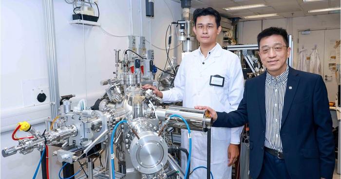
- Image: Prof. Jianhua Hao, (right), Dr. Zehan Wu, (left), and the research team, fabricated ultra-thin heterostructure of 2D bismuth (Bi) and indium selenide (InSe) layers using pulsed laser deposition. (polyu)
PRESS RELEASE — The next generation of microelectronics relies on radical improvements in transistor switching performance to advance computing power. However, conventional semiconductor technology has hit a physical limit known as the “Boltzmann tyranny,” which restricts the energy efficiency of traditional transistors and stalls progress in high-performance electronics. To address this key bottleneck, a research team at The Hong Kong Polytechnic University (PolyU) has engineered a novel tunnelling field-effect transistor (TFET) utilising two-dimensional (2D) nanomaterials. The breakthrough brings this long-awaited experimental technology closer to commercial reality, offering a fundamental building block for energy-efficient computing and next-generation artificial intelligence (AI) chips.
Article Intelligence
Related Coverage
 ResearchMIT Quantum Initiative Launches Postdoctoral Fellowship Programvor 5 Stunden · 3 min read
 ResearchQuantum-Classical Software Tests New Approach to Protein Foldingvor 4 Stunden · 6 min read
 ResearchIQM Award Goes To Researcher Studying Qubit Performancevor 16 Stunden · 3 min read
Sponsored
Ad
NewsLayerLearn more
NewsLayer Premium
Unlock deeper intelligence.
Ad-free reading, exclusive research, and real-time onchain insights.
Go Premium