

Researchers at Friedrich-Alexander-Universität Erlangen-Nürnberg have demonstrated a new approach to controlling silicon vacancy (VSi) qubits by fabricating a lateral pin-diode structure within 4H-SiC, but using the a-plane orientation instead of the conventional c-plane. This alignment positions the VSi dipole moment parallel to the wafer surface, enabling direct optical excitation and facilitating scalable integration with quantum photonic integrated circuits (QPICs).
4H-SiC's A-plane Orientation Simplifies Silicon Vacancy Qubit Control
Researchers at Friedrich-Alexander-Universität Erlangen-Nürnberg have demonstrated a new approach to controlling silicon vacancy (VSi) qubits by fabricating a lateral pin-diode structure within 4H-SiC, but using the a-plane orientation…
Quantum Zeitgeist
Publisher
Nov 13, 2026 at 11:29 AM UTC · Updated 12시간 전 · 7 분 소요
Key Signal
-150 volts Diode blocking capability
Last Updated
12시간 전
번역 중…
The work addresses a critical need for robust, scalable quantum technologies, with potential applications spanning high-precision quantum sensing to scalable quantum computing. This architecture allows for precise electrical Stark tuning of VSi emission frequencies, a core prerequisite for generating indistinguishable photons within a scalable CMOS architecture.
4H-SiC a-Plane Orientation Enables Lateral Pin-Diode Fabrication
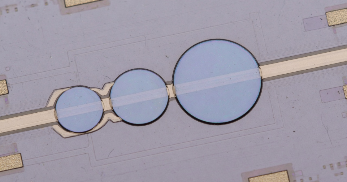
Lateral pin-diodes fabricated on 4H-SiC wafers oriented along the a-plane demonstrate good blocking capabilities up to -150 volts, a critical threshold for minimizing charge noise during sensitive optical measurements. These devices, created using a scalable CMOS process, also exhibit reverse leakage currents below the noise floor of the measurement setup, less than 10 picoamperes, further enhancing signal clarity. The fabrication process successfully integrates silicon vacancy (VSi) defects, positioned as localized spin qubits with robust spin-optical properties, into the diode structure.
Article Intelligence
Topics
Sponsored
Ad
NewsLayerLearn more
NewsLayer Premium
Unlock deeper intelligence.
Ad-free reading, exclusive research, and real-time onchain insights.
Go Premium